SPI Controller Peimplementation in SystemVerilog
2026-02-02 | By Mustahsin Zarif
Previously, we looked at the peripheral side implementation of the Serial Peripheral Interface (SPI) protocol in SystemVerilog, which I claimed to be the easier part of the process. Now, let’s take a closer look at designing the controller in SystemVerilog.
As a reminder, here is the I/O relational diagram of SPI:

I want to make a controller capable of all 4 modes of operation. The mode is decided by the clock polarity and clock phase. Here, the polarity means whether the serial clock idles in the HIGH state or the LOW state, while the phase dictates whether data is sampled on the rising or falling edge.


On the sample edge, we take the bit from the MISO line and put it in a shift register. On the shift edge, we move the next bit in the DATA2SEND register to the MOSI line.
if (sample_edge)

                            shift_reg_in <= {shift_reg_in[6:0], miso}; 		// shift in MISO bit


                        if (shift_edge)

                            shift_reg_out <= {shift_reg_out[6:0], 1'b0}; 		// shift out MISO bit
Let’s set up an enumeration for this:
typedef enum logic [1:0] {

    MODE0 = 2'b00,

    MODE1 = 2'b01,

    MODE2 = 2'b10,

    MODE3 = 2'b11

} spi_mode_t;
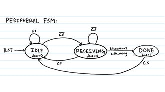
Great. We can work through the FSM transition condition depending on the mode, but let’s first draw the FSM for our design:

typedef enum logic [1:0] {

    IDLE,

    LOAD,

    TRANSFER,

    DONE

} spi_state_t;
This has one extra state than the peripheral. This is because we must load the data to transfer into the shift register whose MSB is reflected on the MOSI bit.
LOAD: begin

                shift_reg_out <= data_to_send;	// temporary register is loaded with the data to be sent to peripheral

                bit_count <= 3'd7; 			// reset bit count for 8 bits

                spi_mode <= spi_mode_t'(mode); 	// set current mode

                sclk_en <= 1'b1; 			// enable SCLK

            end
Now, we can decide how we want to shift and sample bits depending on the SPI mode in the Transfer state:
TRANSFER: begin

                    if (!skip_first_edge) begin

                        if (sample_edge)

                            shift_reg_in <= {shift_reg_in[6:0], miso}; 		// shift in MISO bit


                        if (shift_edge)

                            shift_reg_out <= {shift_reg_out[6:0], 1'b0}; 		// shift out MOSI bit


                        if ((spi_mode == MODE0 || spi_mode == MODE1) && sample_edge ||

                            (spi_mode == MODE2 || spi_mode == MODE3) && shift_edge)

                            bit_count <= bit_count - 1;


                        if (bit_count == 0)

                            skip_last_edge <= 1'b0; 				// reset skip_last_edge after last bit


                    end else skip_first_edge <= 1'b0; 				// reset skip_first_edge after first edge

            end
In the above logic, there are three main points we need to understand:
- skip_first_edge and skip_last_edge: in modes 2 and 3, where the sclk idles high, we need it to go low first before the rising edge can be checked, so we skip the first edge, which is falling. Similarly, once all the data has been transferred, the clock is at a LOW state, but to make it align with the mode, we have to let it transition to HIGH before setting the Chip Select (CS) pin HIGH, so we skip the last edge.
- In modes 0 and 1, the sample happens after shifting, so the bit count is decremented after the sample edge. The opposite is true for modes 2 and 3.
- sample_edge and shift_edge are set using assign statements depending on the SPI mode.
Once the transfer is complete, we move to the DONE state, where we can see the outputs correctly reflecting the values they are supposed to have before moving to the IDLE state that clears all logic.

Now that we understand how to handle the data transfer using FSMs, we can write a module header:
module spi_master #(

    parameter SCLK_DIVIDER = 32

)


(

    input logic clk,

    input logic rst,

    input logic start,
    input logic miso,

    input logic [7:0] data_to_send,

    input logic [1:0] mode,

    output logic mosi,

    output logic sclk,

    output logic cs_n,

    output logic done,

    output logic [7:0] data_received

);
The port list is pretty simple to understand, since it reflects the I/O diagram at the beginning of the blog. The new addition we have to look at is the parameter list: parameter SCLK_DIVIDER = 32. See, your hardware, whether it be an FPGA or an ASIC, has an internal clock that runs at a fixed, high frequency, such as a few megahertz. However, we want our serial clock to operate at a much lower frequency, so we need to divide the clock frequency by the SCLK_DIVIDER to get a smaller operating frequency for the module. All the edges that we want to look at for data control depend on the generated SCLK:
assign rising_edge = sclk & ~sclk_delayed;	// sclk_delayed is the previous value of sclk

assign falling_edge = ~sclk & sclk_delayed;

assign sample_edge = (spi_mode == MODE0 || spi_mode == MODE3) ? rising_edge : falling_edge;

assign shift_edge = (spi_mode == MODE0 || spi_mode == MODE3) ? falling_edge : rising_edge;
 Fig: SCLK operates at a frequency lower than the clock
In order to know how many bits are needed to represent the SCLK_DIVIDER, we can use the $clog2 function:
localparam divider_bits = $clog2(SCLK_DIVIDER);

logic [divider_bits-1:0] clk_divider_count;
________________________________________
We are now near the end of our design. All that is left is to assign the outputs when we reach the DONE state:
DONE: begin

            if (cs_n) begin

                next_state = IDLE; // go back to IDLE when CS is high

            end

        end


        default: next_state = IDLE; // default case to handle unexpected states


assign done = (state == DONE);

assign data_received = shift_reg_in;

assign mosi = shift_reg_out[7];

assign cs_n = (state == IDLE || state == DONE) ? 1'b1 : 1'b0;

assign sclk = sclk_en ? sclk_int : mode[1];
The entire RTL can be found on my GitHub repository for the project, including the testbench used to prove that the design works.
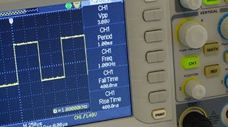
 Fig: SPI Mode 0 waveform
 Fig: SPI Mode 0 waveform showing master receives A5 from the slave as expected when DONE
 Fig: SPI Mode 1 waveform
With this, we have completed an entire SPI design for full-mode functionality! While the previous blog went over the peripheral design, the controller design in this blog explored more complex design considerations that go into making communication protocols for embedded systems. We had to take into account additional FSM states, handle data logic based on how the clock polarity and phase are used, and generate our own clock. Finally, to make sure our hard work resulted in success, we ran simulations to visually inspect the dataflow waveform and adjust any errors accordingly.