The Smith Chart: An ‘Ancient’ Graphical Tool Still Vital in RF Design
Electronic Products の提供
2014-03-06
The Smith chart is a valuable and often essential tool for anyone dealing with impedance issues in wired and wireless design at RF frequencies. It was developed in the 1930s by Phillip Hagar Smith at Bell Telephone Laboratories, who wrestled with the problem of how to show and evaluate multiple complex impedance parameters (which can range from zero to infinity) on a two-dimensional bounded graph. Its first public presentation was in a 1939 issue of Electronics magazine. (Note that "Smith chart" is a registered trademark of Analog Instruments Company of New Providence, NJ.)
Although the Smith chart is one of the oldest tools in the RF kit, it is by no means obsolete, and is still used extensively in hands-on aspects of engineering. While paper and pencil versions of it are, of course, less common than in the past, many datasheets and analysis and modeling application programs present data in Smith chart form. So does test equipment; it is also used extensively in RF/microwave network analyzers. (Also note that the Smith chart can be used to graph multiport scattering parameters (S-parameters S11, S12, S22, S21), a standard tool for characterizing devices using vector network analysis, but that is another, much more complicated story.)
In RF circuits, matching the impedance between a source and load is critical to achieve effective power transfer with minimal loss, and avoid standing waves and reflections on transmission lines arising from the signal energy impinging on any impedance discontinuity. This is no longer just an "RF designer" issue, as the increase in clock speed of today's digital circuits, many are in the gigahertz range, means that the "pure" digital signals are actually in the RF domain. Therefore, analog real-world considerations, such as impedance and line/load matching, come into the picture. The Smith chart is used to assess the signal path from PC board contact pad to the lead or pad of a device such as an IC, transistor, or passive component, and internal circuitry of the device.
The Smith chart is most commonly used to display the resistive and reactive portions of a component’s complex impedance (z = ∞R + jX) versus frequency, and then use this to develop a matching circuit between the component and a driver or load. It can also be used to ascertain the locus of a component’s impedance versus frequency, needed to perform stability analysis and avoid (or sustain) oscillation.
While it is possible with today’s high-speed PCs and instrumentation to display the relevant impedances numerically as table or list, the chart allows visualization of impedance, transitions, and options for getting from Point A to Point B. Such visualizations are more revealing and indicative of the situation and tradeoffs the designer faces.
A look at the Smith chart
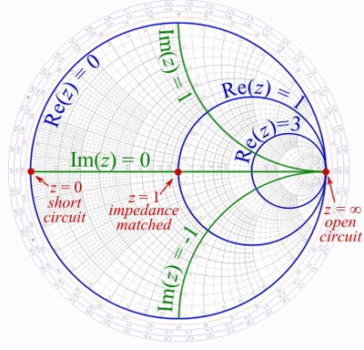
The Smith chart is both graphically simple and complex at the same time. A full chart has many gradations and arcs, but if you remove these, you can see the basic underpinnings of its two sets of curves (Figure 1). The simplified chart calls out two numerical values of real impedance and imaginary impedance, along with key delineation points, for relative comparison.

Figure 1: The basic graphical elements of the Smith chart are circles that touch at a point on the right-hand side to represent real part R of a complex impedance z = R + jX, and arcs.
All the circles on the right-hand side touch at the extreme right, with circles of increasing diameter corresponding to increases in the value of resistance R (the real part of the impedance); all points on a given circle have the same R value. The point at which all the circles touch is for impedance z = ∞ (an open circuit); the opposite left-hand point is for z = 0 Ω (an open circuit).
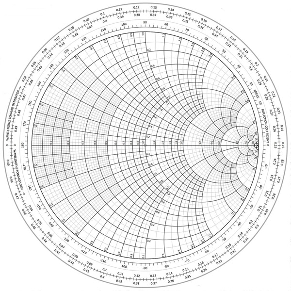
For the reactive (imaginary) part of the impedance, the chart uses arcs that originate on the right-hand side; all points on a given arc have the same reactance value. For reactance, arcs in the upper half correspond to inductive reactance (+jX) while those in the lower half correspond to capacitive reactance (-jX). Although this approach may seem somewhat obvious in retrospect, it took Smith several years to develop this chart and understand how it could be used, with the help of several associates who were experts in conformal mapping techniques. An “official” Smith chart has a more gradations and detail (Figure 2).
Figure 2: The complete, standard Smith chart is a more detailed version of the basic one, but has the same topographical structure and elements.
There is yet another capability of the chart based on centered, concentric circles (not to be confused with the resistance circles which touch the right-hand side). The boundary of each circle represents points of equal VSWR (vertical standing wave ratio, a key parameter for matching and assessing loss and reflections), with larger circles indicating higher VSWR.
Impedances can range anywhere from 0 to large and even near-infinite numbers. How does the chart handle this? It uses the standard technique of normalization, where you scale the values versus the nominal impedance Z0 you are using (usually 50 Ω). Therefore, for a measured impedance of 125 + j100 Ω, you would divide by 50 and the normalized value to plot is 2.5 +j2 Ω. When you are done, you simply rescale accordingly.
Using the Smith chart
Graphing an impedance or set of impedances versus frequency on the chart is fairly straightforward. However, using the Smith chart to match source and load, determine admittance (the inverse of complex impedance, and needed to work out so-called stub tuning), characterize transmission lines, and assess stability criteria is not easy, though the chart makes it much easier than alternative methods. You will need instruction from books and videos, plus practice and patience (just Google "Smith chart" and “YouTube” and you will see many videos, each just a few minutes long; also see the many listed references with this article.)
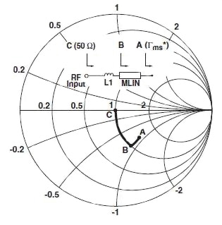
Since the Smith chart is both useful and universal, many component and subsystem vendors include it on their datasheets along with other specifications and performance graphs. The datasheet for the Avago Technologies MGA-83563 (a 22 dBm PSAT 3 V power amplifier for 0.5 to 6 GHz applications) provides both a table of S-parameters and a Smith chart. It uses these two tools to work out a matching circuit between the drive circuit and the input of the amplifier (Figure 3), showing how the addition of a 0.15 in. length of FR-4 PC board material as a 50 Ω transmission line rotates Point A around to Point B on the R = 1 circle of the Smith chart.

Figure 3: The datasheet for the Avago Technologies MGA-83563 RF PA shows an example of using the Smith chart for developing a matching circuit between a driver and the PA input.
A series 2.5 nH inductor (L1) is then all that is required to complete the match to 50 Ω at Point C as shown in the schematic (Figure 4).

Figure 4: A series 2.5 nH inductor (L1).
Summary
The Smith chart is a graphical tool used extensively for wired and wireless design at RF frequencies. It is used to express and analyze the impedance of electronic components versus the operating frequency. This article examined the basics of the Smith chart, what it shows, and why it is useful. An example using the Avago Technologies MGS-83563 RF power amplifier explained how it is used for impedance matching between a source and load.
Further reading:
Smith chart:
- http://en.wikipedia.org/wiki/Smith_chart
- Smith Chart tutorial
- Introduction to Smith Charts
- Smith Chart basics
- http://www.microwaves101.com/encyclopedia/sparameters.cfm
- http://en.wikipedia.org/wiki/Scattering_parameters
免責条項:このウェブサイト上で、さまざまな著者および/またはフォーラム参加者によって表明された意見、信念や視点は、DigiKeyの意見、信念および視点またはDigiKeyの公式な方針を必ずしも反映するものではありません。


